
VIP member

E83-2G4M03S nRF5340 chip Bluetooth mesh wireless module
Communication protocol: BLE 5.2
Product details



| Main application | performance | notes | |
| minimum value | Maximum value | ||
| supply voltage(V) | 1.7 | 5.5 | Module permanently burned out beyond 5.5V |
| Blocking power (dBm) | - | 10 | The probability of burning is relatively low when used at close range |
| operation temperature(℃) | -40 | 105 | Industrial grade |
| Main application | performance | notes | |||
| minimum value | Typical values | Maximum value | |||
| Voltage Mode | Normal voltage mode | 1.7 | 3.3 | 3.6 | ≥ 3.3V ensures output power |
| High voltage mode | 2.5 | 5 | 5.5 | - | |
| Communication level(V) | - | 3.3 | - | There is a risk of burning out when using 5V TTL | |
| Working temperature (℃)) | -40 | - | 105 | Industrial grade design | |
| Working frequency band (MHz) | 2360 | - | 2500 | Support ISM frequency band | |
|
send out shoot electricity flow |
TX only run current (DC/DC, 3 V) PRF = +3 dBm |
- | 5.1 | - | mA |
| TX only run current PRF = +3 dBm | - | 12.44 | - | mA | |
| TX only run current (DC/DC, 3 V)PRF = 0 dBm |
- | 3.7 | - | mA | |
| TX only run current PRF = 0 dBm | - | 9.1 | - | mA | |
|
connect put away electricity flow |
RX only run current (DC/DC, 3 V) 1 Mbps/1Mbps BLE |
- | 2.7 | - | mA |
| RX only run current LDO,3V, l Mbps / 1 Mbps BLE |
- | 6.7 | - | mA | |
| RX only run current (DC/DC, 3 V) 2Mbps/2 Mbps BLE |
- | 3.1 | - | mA | |
| RX only run current LDO,3V, 2 Mbps / 2 Mbps BLE |
- | 7.9 | - | mA | |
| Low power consumption current | - | 0.7 | - | uA | |
| Transmission power (dBm) | - |
0 |
3 | dBm | |
| Receiving sensitivity (dBm) | -104dBm @ BLE 125kbps | Long distance mode | |||
| -98dBm @ BLE 1Mbps | - | ||||
| Parameters | describe | notes |
| Reference distance | 170m | Transmission power 0dBm,Clear and open environment, antenna gain5dBi,height25Meter, air speed1Mbps |
| Vibration frequency | 32MHz/32.768KHz | - |
| support agreement | BLE 5.2 | - |
| communication interface |
IO |
- |
| Packaging method | Surface mount type | - |
| Full name of IC | nRF5340-QKAA/aQFN ™ ninety-four | - |
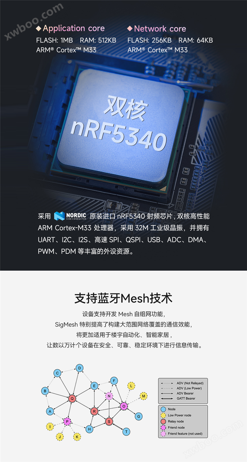
| FLASH | 1 M | - |
| RAM | 512KB | - |
| kernel | Dual core 128/64 MHz ARM ® Cortex ® - M33 | - |
| External dimensions | 16.0 * 16.0mm | 0.1mm |
| antenna interface | 1st generation IPEX | Equivalent ImpedanceAbout 50Ω |
| Product weight | 1.2g | 0.1g |

| Pin number | Pin Name | Pin direction | Pin usage |
| 1 | RESET | input | Special pins for external reset (see nRF5340 manual for details) |
| 2 | SWDIO | Input 1 Output | Serial debugging interface, serial data input and output (see nRF534O manual for details) |
| 3 | SWDCLK | input/output | Serial debugging interface, serial line clock (see nRF5340 manual for details) |
| 4 | P1.10 | Input 1 Output | Configurable universal IO port (see nRF5340 manual for details) |
| 5 | P0.31 | input/output | Configurable universal IO port (see nRF5340 manual for details) |
| 6 | P1.12 | Input 1 Output | Configurable universal IO port (see nRF5340 manual for details) |
| 7 | P1.14 | input/output | Configurable universal IO port (see nRF5340 manual for details) |
| 8 | P0.04/AIN0 | input/output | Configurable universal IO port; Can simulate input (see nRF5340 manual for details) |
| 9 | D+ | input/output | USB D+; Connect the D+data cable directly to the UBS bus (see nRF5340 manual for details) |
| 10 | VBUS | input | USB power supply, range 4.35V-5.5V (see nRF5340 manual for details) |
| 11 | P0.28/AIN7 | input/output | Configurable universal IO port; Can simulate input (see nRF5340 manual for details) |
| 12 | GND | - | Ground wire, connected to the power reference ground |
| 13 | P0.29 | input/output | Configurable universal IO port (see nRF5340 manual for details) |
| 14 | P0.30 | input/output | Configurable universal IO port (see nRF5340 manual for details) |
| 15 | P1.11 | input/output | Configurable universal IO port (see nRF5340 manual for details) |
| 16 | P1.13 | input/output | Configurable universal IO port (see nRF5340 manual for details) |
| 17 | P1.15 | input/output | Configurable universal IO port (see nRF5340 manual for details) |
| 18 | D- | input/output | USB D-: Directly connect the D-data line to the UBS bus (see nRF5340 manual for details) |
| 19 | GND | - | Ground wire, connected to the power reference ground |
| 20 | GND | - | Ground wire, connected to the power reference ground |
| 21 | VDD_HV | input | Power supply, range 2.5V-5.5V (see nRF5340 manual for details) |
| 22 | GND | - | Ground wire, connected to the power reference ground |
| 23 | VDD_nRF | input | Power supply, range 1.7V-3.6V (see nRF5340 manual for details) |
| 24 | GND | - | Ground wire, connected to the power reference ground |
| 25 | P0.00/XL1 | input/output | Configurable universal IO port; Can connect to a 32KHz crystal oscillator (see nRF5340 manual for details) |
| 26 | P0.01/XL2 | input/output | Configurable universal IO port; Can connect to a 32KHz crystal oscillator (see nRF5340 manual for details) |
| 27 | P0.02/NFC1 | input/output | Configurable universal IO port; NFC antenna interface (see nRF5340 manual for details) |
| 28 | P0.03/NFC2 | input/output | Configurable universal IO port; NFC antenna interface (see nRF5340 manual for details) |
| 29 | P1.01 | input/output | Configurable universal IO port (see nRF5340 manual for details) |
| 30 | P1.00 | input/output | Configurable universal IO port (see nRF5340 manual for details) |
| 31 | P1.05/AIN1 | input/output | Configurable universal IO port; Can simulate input (see nRF5340 manual for details) |
| 32 | P1.06/AIN2 | input/output | Configurable universal IO port; Can simulate input (see nRF5340 manual for details) |
| 33 | PI.07/AIN3 | input/output | Configurable universal IO port; Can simulate input (see nRF5340 manual for details) |
| 34 | P1.03/I²C | input/output | Configurable universal IO port; I ² C bus interface (see nRF5340 manual for details) |
| 35 | P1.02/I²C | input/output | Configurable universal IO port; I ² C bus interface (see nRF5340 manual for details) |
| 36 | P0.08/TRACEDATA3/SCK | input/output | Configurable universal IO port; Tracking buffer TRACEDATA [3]; SPIM4 (see nRF5340 manual for details) |
| 37 | P0.09/TRACEDATA2/MOSI | input/output | Configurable universal IO port; Tracking buffer TRACEDATA [2]; SPIM4 (see nRF5340 manual for details) |
| 38 | P0.10/TRACEDATA1/MISO | input/output | Configurable universal IO port; Tracking buffer TRACEDATA [1]; SPIM4 (see nRF5340 manual for details) |
| 39 | P0.11/TRACEDATA0/CSN | input/output | Configurable universal IO port; Tracking buffer TRACEDATA [0]; SPIM4 (see nRF5340 manual for details) |
| 40 | P0.13/QSPI0 | input/output | Configurable universal IO port; Queue serial peripheral interface QSPI; (See nRF5340 manual for details) |
| 41 | P0.19 | input/output | Configurable universal IO port (see nRF5340 manual for details) |
| 42 | P1.04 | input/output | Configurable universal IO port (see nRF5340 manual for details) |
| 43 | P1.08 | input/output | Configurable universal IO port (see nRF5340 manual for details) |
| 44 | P0.20 | input/output | Configurable universal IO port (see nRF5340 manual for details) |
| 45 | P0.26/AIN5 | input/output | Configurable universal IO port; Can simulate input (see nRF5340 manual for details) |
| 46 | GND | - | Ground wire, connected to the power reference ground |
| 47 | GND | - | Ground wire, connected to the power reference ground |
| 48 | P0.12/TRACECLK/DCX | input/output | Configurable universal IO port; Tracking buffer clock; SPIM4 (see nRF5340 manual for details) |
| 49 | P0.16/QSPI3 | input/output | Configurable universal IO port; Queue serial peripheral interface QSPI; (See nRF5340 manual for details) |
| 50 | P0.21 | input/output | Configurable universal IO port (see nRF5340 manual for details) |
| 51 | P1.06 | input/output | Configurable universal IO port (see nRF5340 manual for details) |
| 52 | P0.14/QSPI1 | input/output | Configurable universal IO port; Queue serial peripheral interface QSPI; (See nRF5340 manual for details) |
| 53 | P0.24 | input/output | Configurable universal IO port (see nRF5340 manual for details) |
| 54 | P0.22 | input/output | Configurable universal IO port (see nRF5340 manual for details) |
| 55 | GND | - | Ground wire, connected to the power reference ground |
| 56 | GND | - | Ground wire, connected to the power reference ground |
| 57 | P0.23 | input/output | Configurable universal IO port (see nRF5340 manual for details) |
| 58 | P1.05 | input/output | Configurable universal IO port (see nRF5340 manual for details) |
| 59 | P0.25/AIN4 | input/output | Configurable universal IO port; Can simulate input (see nRF5340 manual for details) |
| 60 | P0.27/AIN6 | input/output | Configurable universal IO port; Can simulate input (see nRF5340 manual for details) |
| 61 | P0.17/QSPI_CLK | input/output | Configurable universal IO port; Queue serial peripheral interface QSPI; (See nRF5340 manual for details) |
| 62 | P0.15/QSPI2 | input/output | Configurable universal IO port; Queue serial peripheral interface QSPI; (See nRF5340 manual for details) |
| 63 | P0.18/QSPI_CS | input/output | Configurable universal IO port; Queue Serial Peripheral Interface QSPI Please refer to the nRF5340 manual for details |
| 64 | P1.09 | input/output | Configurable universal IO port (see nRF5340 manual for details) |
| 65 | P1.07 | input/output | Configurable universal IO port (see nRF5340 manual for details) |
|
Product manual |
|
|
|
Development testing |
|
Introduction to Yibaite |
|
|
|
Online purchase |
|
Yibaite Official Taobao Store: |
|
To Zhe Yi Bai Te Exclusive Store: |
|
Alibaba: |
|
Bulk procurement/customized products |
|
Sales Hotline: 7x24 hour sales service hotline |
|
[Contact email]: sales@cdebyte.com |
|
Technical Consultation |
|
Online submission: |
|
[Contact email]:support@cdebyte.com |
| product model |
interface type | Chip Solution | Carrier frequency Hz | Transmission power dBm | Test distance in kilometers | communication protocol | antenna form | Product size mm | Product Features | technology manual |
sample buy |
|---|---|---|---|---|---|---|---|---|---|---|---|
| SoC | nRF5340 | 2360~2500M | 3 | 0.17 | BLE 5.2 | IPEX | 16*16 | Small size and low power consumption |
-
E83-2G4M03S
Product model: E83-2G4M03S
interface type
: SoC
Chip Solution
: nRF5340
Carrier frequency Hz
: 2360~2500M
Transmission power dBm
: three
Test distance in kilometers
: zero point one seven
communication protocol
Online inquiry
-
Contacts
-
Company
-
Telephone
-
Email
-
WeChat
-
Verification Code
-
Message Content
-